
Saturday, 15 July 2017
Thursday, 6 July 2017
XILINX ISE DESIGN SUIT 10.1 VERSION PRACTICE TUTORIAL
SOFTWARE REQUIREMENT XILINX ISE DESIGN SUITE 10.1 VERSION
HARDWARE REQUIREMENT:
PERSONAL COMPUTER
SPARTAN 3E(XC3S100E)
BUSES
This is the way to do project practice simple for beginner to excellent learning from this blog . i can explain clearly about to do project in VLSI by using verilog coding WITH GOOD EXAMPLES
There are two ways i can give code for every module in hardware description lanuage (HDL) and similarly in verilog and system verilog also.
let we start from one way to go for another way for practice first and do more projects on it .
COMPUTATIONAL CIRCUITS AND SEQUENTIAL CIRCUITS
COMPUTATIONAL CIRCUITS
GATES
ADDERS
HALF ADDER
FULL ADDER
RIPPLE CARRY ADDER.
CARY LOOK AHEAD ADDER
MULTIPLEXER
(4X1)
(8X1)
(16X1)
DEMULTIPLEXERS
(1X4)
(1X8)
(1X16)
DECODER (2 TO 4)
(3 TO 8)
(4 TO 16)
SEQUENTIAL CIRCUITS
FLIP FLOPS
RS FLIP FLOPS
JK FLIP FLOPS
D FLIP FLOPS
T FLIP FLOPS
COUNTERS
4-BIT COUNTER
8-BIT COUNTER
DECADE COUNTER
UP/DOWN COUNTER
RING COUNTER
JHONSON COUNTER
REGISTERS
SHIFT REGISTER
SISO REGISTER
PIPO REGISTER
ALU
FAGA
ASIC
Wednesday, 5 July 2017
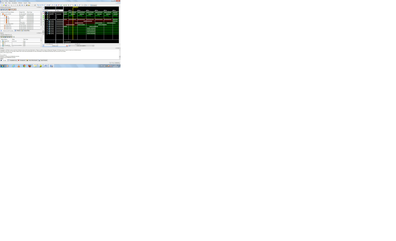
VERILOG AND HDL DESIGN WITH FLOW CHART AND EXAMPLE
FPGA demonstrates good
performance and logic capacity by exploiting parallelism. At present single
FPGA platform can play multi-functions, including control, filter and system. FPGA
design flow is a three-step process consisting of design entry, implementation,
and verification stages, as shown in Fig 2.1.The full design flow is an
iterative process of entering, implementing, and verifying the design until it
is correct and complete.
Verilog HDL
is a hardware description language used to design and document electronic
systems. Verilog HDL allows designers to design at various levels of abstraction
Verilog HDL originated at Automated Integrated Design
Systems (later renamed as Gateway Design Automation) in 1985. The company was
privately held at that time by Dr. Prabhu Goel, the inventor of the PODEM test
generation algorithm. Verilog HDL was designed by Phil Moorby, who was later to
become the Chief Designer for Verilog-XL and the first Corporate Fellow at
Cadence Design Systems. Gateway Design Automation grew rapidly with the success of
Verilog-XL and was finally acquired by Cadence Design Systems, San Jose, CA in
1989.
Verilog was invented as simulation language. Use of
Verilog for synthesis was a complete afterthought. Rumors abound that there
were merger discussions between Gateway and Synopsys in the early days, where
neither gave the other much chance of success.
VERILOG is fully
simulatable, but not fully synthesizable. There are several VERILOG constructs
that do not have valid representation in a digital circuit. Other constructs
do, in theory, have a representation in a digital circuit, but cannot be
reproduced with guaranteed accuracy. Delay time modeling in VERILOG is an
example. State-of-the-art synthesis algorithms can optimize Register Transfer
Level (RTL) circuit descriptions and target a specific technology. Scheduling
and allocation algorithms, which perform circuit optimization at a very high
and abstract level, are not yet robust enough for general circuit
applications. Therefore, the result of synthesizing a VERILOG description
depends on the style of VERILOG that is used.
In Verilog minute errors won’t
popup during the compilation time. It will pop up at the time of synthesis
only. The Verilog language is still rooted in its native interpretative mode.
Compilation is a means of speeding up simulation, but has not changed the
original nature of the language. As a result care must be taken with both the compilation
order of code written in a single file and the compilation order of multiple
files. Simulation results can change by simply changing the order of
compilation.
There is no equivalent to the generate statement in Verilog. Signals
representing objects of different bits widths may be assigned to each other.
The signal representing the smaller number of bits is automatically padded out
to that of the larger number of bits, and is independent of whether it is the
assigned signal or not. Unused bits will be automatically optimized away during
the synthesis process. This has the advantage of not needing to model quite so
explicitly as in VHDL, but does mean unintended modeling errors will not be
identified by an analyzer.
The standard design flow
comprises the following steps:
Ø Design Entry and
Synthesis: In this step of the design flow, design
is created using a, a hardware description language (HDL) for text-based entry.
Xilinx Synthesis Technology (XST) GUI can be used to synthesize the HDL file
into an NGC file.
Ø Design Implementation:
By implementing to a specific Xilinx architecture, the logical design file
format, such as EDIF, that is created in the design entry and synthesis stage
is converted into a physical file format. The physical information is contained
in the native circuit description (NCD) file for FPGAs Then bit stream file is
created from these files and optionally a PROM or EPROM is programmed for
subsequent programming of Xilinx device.
Ø Design Verification:
Using a gate-level simulator or cable, it is ensured that the design meets
timing requirements and functions properly.
To define the behavior of the FPGA, the user provides a
hardware description language (HDL) or a schematic design. The HDL form is more suited to work with large structures
because it's possible to just specify them numerically rather than having to draw
every piece by hand. However, schematic entry can allow for easier
visualization of a design. Then, using an electronic design automation tool, a technology-mapped net list is generated. The net list can then be fitted to the actual FPGA
architecture using a process called place-and-route, usually performed by the FPGA Company’s proprietary
place-and-route software.
The various steps involved in the design flow
are as follows:
1) The design
2] Processes and properties
3] Synthesize options
4] Write Timing Constraints
5) Timing simulation of the
design after post PAR.
6) Static timing analysis.
7) Configuring the device by bit generation.
Ø Design entry
The first step in implementing the design is to create the HDL code
based on design criteria. To support these instantiations we need to include
UNISIM library and compile all design libraries before performing the
functional simulation. The constraints (timing and area constraints) can also
be included during the design entry. Xilinx accepts the constraints in the form
of user constraint (UCF) file.
Ø Functional Simulation
This step deals with the verification of the functionality of the
written source code. ISE provides its own ISE simulator and also allows for the
integration with other tools such as ModelSim. This project uses ModelSim for the ise. Functional simulation can
take place at the earliest stages of the design flow. Because timing
information for the implemented design is not available at this stage, the
simulator tests the logic in the design using unit delays.
Ø Synthesizing and
Optimizing
In this stage behavioral information in the HDL file is translated
into a fed into the Xilinx software program called NGD Build, which produces a
logical native generic database
(NGD) file.
Ø Design implementation
In this stage, The MAP
program maps a logical design to a Xilinx FPGA. The input to MAP is an NGD
file, which is generated using the NGD Build Xilinx primitives. The NGD file
also contains any number of NMC (macro library) files, each of which contains
the definition of a physical macro. MAP first performs a logical DRC (Design
Rule Check) on the design in the NGD file. MAP then maps the design logic to
the components (logic cells, I/O cells, and other components) in the target
Xilinx FPGA The output from MAP is an NCD (Native Circuit Description) file,
and PCF (Physical constraint file).
Ø Timing
simulation after post PAR
Timing simulation at this stage verifies that the design runs at
the desired speed for the device under worst-case conditions. This process is
performed after the design. It can also determine whether or not the design
contains set-up or hold violations. In most of the designs the same test bench
can be used to simulate at this stage.
Ø Static
timing analysis
Static timing analysis is
best for quick timing checks of a design after it is placed and routed. It also
allows you to determine path delays in your design. Following are the two major
goals of static timing analysis:
• Timing verification:-This is verifying that
the design meets your timing constraints.
•
Reporting:-This is enumerating input constraint violations and placing them
into an accessible TRACE are .ncd file and .pcf from PAR .and the output file
is a .twr file.
Ø Configuring the device
by BitGen
After the design is completely routed, it is necessary to configure
the device so that it the configuration information from the NCD file that
defines the internal logic and interconnections of the FPGA, plus
device-specific information from other files associated with the target device.
The binary data in the BIT file is then downloaded into the FPGAs memory cells,
or it is used to create a PROM file.
2.6.1
Processes
and properties
Processes and properties enable the interaction of our design with
the functionality available in the ISE™ suite of tools.
Ø Processes
Processes are the functions listed hierarchically in the Processes
window. They perform functions from the start to the end of the design flow.
Ø Properties
Process properties are accessible from the
right-click menu for select processes. They enable us to customize the
parameters used by the process. Process properties are set at synthesis and
implementation phase.
2.6.2
Synthesize
options:
The following properties
apply to the Synthesize properties .using the Xilinx® Synthesis Technology
(XST) synthesis tool.
The drop-down list.
Speed:-Optimizes the design
for speed by reducing the levels of logic.
Area:-property is set to Speed.
Ø Optimization Effort
Specifies the synthesis
optimization effort level.
Select an option from the
drop-down list.
Normal: - Optimizes the design using
minimization and algebraic factoring algorithms.
High: - Performs additional optimizations that
are tuned to the selected device
Normal:
- This project aims at Timing performance and was selected HIGH effort level.
Ø Power Reduction
When set to is set to No (checkbox is blank).
Ø Use Synthesis
Constraints File: Specifies whether or
not to use the constraints file entered in the previous property. By default,
this constraints file is used (property checkbox is checked).
Ø Keep Hierarchy: Specifies
whether or not the corresponding design unit should be preserved and not merged
with the rest of the design. You can specify Yes, No and Soft property from no
to yes give me almost doubles the speed.
Ø Global Optimization
Goal: Specifies the global timing optimization
goal Select Optimizes the maximum delay from input pad to clock, either for a
specific clock or for an entire design. Offset Out After Optimizes the maximum
delay from clock to output pad, either for a specific is set to All Clock Nets.
Ø Generate RTL Schematic:
Generates a pre-optimization RTL
schematic of the design. Values for this property are Yes, No, and only. Only
stops the synthesis process before optimization, after the RTL schematic has
been generated. The default value is yes.
Ø Read Cores: Specifies
whether or not black box core are read for timing and area estimation (checkbox
is blank), cores are not read. By default, this property is set to True
(checkbox is checked).
2.6.3
Write
Timing Constraints (FPGA only)
Specifies
whether or not to place timing constraints in the NGC file. The timing
constraints in the NGC file will be used during place and route, as well as
synthesis optimization. By default, this property is set to False (checkbox is
blank).
Ø Slice Utilization Ratio:
Specifies resource management by
entering -1 here.
Ø LUT-FF Pairs
Utilization Ratio: Specifies the area size
(in %) that XST will not exceed during timing optimization. If the
resource management by entering-1 here.
Ø BRAM Utilization Ratio
Specifies the number of BRAM blocks (in %) that
XST will not exceed during synthesis. The default percentage is 100%. You can
disable automatic BRAM resource management by entering -1 here.
2.6.4
Implementation
Options
Perform Timing-Driven Packing
and Placement Specifies whether or not to give priority to timing critical
paths during packing in the Map Process. User-generated timing constraints are
used to result is a completely placed design, and the design is ready for
routing. If Timing-Driven Packing and Placement is selected in the absence of
user timing constraints, the tools will automatically generate and dynamically
adjust timing constraints for all internal clocks. This feature is referred to
as “achieve. Instead it is a “balance” of performance between all clocks in the
design. By default, this property is set to False (checkbox is blank).This
project aims at speed and this option is selected.
Ø Map Effort Level: Note: Available only
when Perform Timing-Driven Packing and Placement is set to True (checkbox is
checked). Specifies the effort level to apply to the Map process. The effort
level controls the amount of time used for packing and placement by selecting a
more or less CPU-intensive algorithm for placement. Select an Gives the longest
run time with the best mapping results. Appropriate for a more complex design.
By default, this property is set to Medium. As this project is a complex design
the option high is selected.
Ø Extra Effort: Map
is applied. Normal R-uns until timing constraints are met unless they are found
to be impossible to meet. This option focuses on meeting timing constraints. This
project has a timing constraint of 100 ns; to meet this option Normal is
selected.
2.6.5
Combinatorial
Logic Optimization: Specifies whether or
not to run a process that revisits the combinatorial design. This project aims
to meet timing constraint and this option is selected.
2.6.6
Optimization
Strategy (Cover Mode)
Specifies
the criteria used during the "cover" phase of MAP. In the
"cover" phase, MAP assigns the logic to CLB function generators
(LUTs). Select an option from the drop-down list.
Ø Area: Select
Area to make reducing the number of LUTs (and therefore the number of CLBs) the
highest priority.
Ø Speed: Select
Speed to make reducing the number of levels of LUTS (the number of LUTs a path
passes through) the highest priority. This setting makes it the area setting),
and in some cases the increase may be large.
Ø Balanced: Select
Balanced to balance two priorities; reducing the number of LUTs and reducing
the number of levels of LUTs. The Balanced option produces results
Ø Optimization: By
default, this property is set to Area. To meet timing constraints this project
selected the option of speed.
2.6.7
PAR
properties
Ø Place and Route Effort
Level (Overall)
Specifies CPU-intensive
algorithm for placement and routing. You can set the overall level from
Standard (fastest run time) to High (best results). By default, this property
is set at Standard. To meet the timing constraint HIGH is selected for this
project.


MATHEMATICS FOR TENTH CLASS STUDENTS
MATHEMATICS FOR TENTH CLASS STUDENTS
Here I am giving the information about tenth class mathematics for new syllabus with detailed analysts for whom studying tenth class students in India, i can make some tricks to find out answer to solve problem in particular manner, here i introduce new methods for mathematics tricks and tips.

in the above picture we are giving the information part -1 as paper -1 for main exam prepare for the best to start in series of Real Numbers and SETS and Progression and Polynomial Remain two chapters are give choice to learn of one lesson and give more importance to learn to get high score in mathematics

in the above picture we are giving the information part -2 as paper -2 for main exam prepare for the best to start in series of trigonometry more importance and application trigonometry statistics second importance and mensuration and coordinate geometry.
further information going to update as soon as possible and regularly
we can follow daily this web page we give require information about tenth class mathematics for preparation daily for main exam tips and exam regularly
day-2
today we are going to learn about one chapter in mathematics of tenth class. so clearly observe this topics as explain in three ways one that of text formation and clearly read what i am saying in this chapter and second way to explain ppt you can download my ppt and go full view and learn one page to another by clicking or press enter.
finally i am going to give you one video for explain of one chapter today.
REAL NUMBERS
Real number are number which can be classified to different and there are different types of numbers to be classified as rational number, even numbers, odd numbers, prime numbers, composite numbers, irrational numbers and whole numbers etc....
Even numbers:
Even number are which number is factor of two and if we divisible by two the remainder is zero and similarly the number which is giving serially two half by the number with great factor.
for example we going to say one number we can easily recognize that is even or not because in the lower class we are already to learn about even number and practice so much.
EXAMPLE: 2,4,6,8,10,12,14,16,18,20,22,24,26,28,30,32,34,36,38 AND etc............
Q. which is even number in the following number ?
a) 5 b)6 c)7 d)8 e) b & d f) a & c
answer: e
Q. in the following number which number is even ?
a) 254 b)524803 c)432578 d)524501 e) a & c f) b&d
answer : e
2222222 20456 246802
4444444 45678 468024
6666666 67802 684206
8888888 80246 826428
in the above numbers have one even number every number can be divisible by two and remainder is zero for every number and any of these number even in five digits or 6 digits or 4 digit or any number of digits can be divisible by two it can get result as remainder as zero that number is known as EVEN number.
Thursday, 6 August 2015
AP Loan Status Of III phase of farmer
AP Loan Status Of III phase of farmer
this was real loan status of the farmer loan debit of you account in the loan with you Aadhar and Rationa Card and loan account number serach with bank loan details was displayed on the screen with below link of every person know what is the status of loan account deducted by the government as per the rule of go's from the cm Chandra babu Naidu and his team released the status of loan account of III phase for the long period of sequence
click here the below link for the loan status check the loan of you account with the aadhar and ration card and loan account no;
Wednesday, 15 July 2015
C PROGRAMMING AND DATA STUCTURE
C PROGRAMMING AND DATA STRUCTURE
- It is a data Structure which consists if group of nodes that forms a sequence.
- It is very common data structure that is used to create tree,graph and other abstract data types.
| No | Element | Explanation |
|---|---|---|
| 1 | Node | Linked list is collection of number of nodes |
| 2 | Address Field in Node | Address field in node is used to keep address of next node |
| 3 | Data Field in Node | Data field in node is used to hold data inside linked list. |
Advantages of linked list

List of advantages :
- Linked List is Dynamic data Structure .
- Linked List can grow and shrink during run time.
- Insertion and Deletion Operations are Easier
- Efficient Memory Utilization ,i.e no need to pre-allocate memory
- Faster Access time,can be expanded in constant time without memory overhead
- Linear Data Structures such as Stack,Queue can be easily implemeted using Linked list
- llocate as much memory as we can.
- Though you can allocate any number of nodes, still there is limit for allocation of memory . (We can allocate memory considering that heap size will not be exceeded)
Re-commanded article : Dynamic memory allocation
2. Insertion and Deletion Operations are easy
- Insertion and Deletion operations in Linked List is very flexible.
- We can insert any node at any place easily and similarly we can remove it easily.
- We don’t have to shift nodes like array insertion. In Insertion operation in linked list , we have to just update next link of node.
3. Memory Utilization
- As explained earlier we don’t have to allocate memory at compile time.
- Memory is allocated at run time as per requirement, so that Linked list data structure provides us strong command on memory utilization.
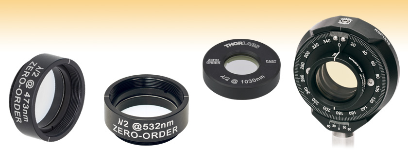
QUATER AND HALF WAVE PLATES
QUARTER AND HALF WAVE PLATES
Waveplate
A waveplate or retarder is an optical device that alters the polarization state of a light wave travelling through it. Two common types of waveplates are the half-wave plate, which shifts the polarization direction of linearly polarized light, and thequarter-wave plate, which converts linearly polarized light into circularly polarized light and vice versa.[1] A quarter wave plate can be used to produce elliptical polarization as well.


Principles of operation
A waveplate works by shifting the phase between two perpendicular polarization components of the light wave. A typical waveplate is simply a birefringent crystal with a carefully chosen orientation and thickness. The crystal is cut into a plate, with the orientation of the cut chosen so that the optic axis of the crystal is parallel to the surfaces of the plate. This results in two axes in the plane of the cut: the ordinary axis, with index of refraction no, and the extraordinary axis, with index of refraction ne. The ordinary axis is perpendicular to the optic axis. The extraordinary axis is parallel to the optic axis. For a light wave normally incident upon the plate, polarization component along the ordinary axis travels through the crystal with a speed vo = c/no, while the polarization component along the extraordinary axis travels with a speed ve = c/ne. This leads to a phase difference between the two components as they exit the crystal. When ne < no, as in calcite, the extraordinary axis is called the fast axis and the ordinary axis is called the slow axis. For ne > no the situation is reversed.
Depending on the thickness of the crystal, light with polarization components along both axes will emerge in a different polarization state. The waveplate is characterized by the amount of relative phase, Γ, that it imparts on the two components, which is related to the birefringence Δn and the thickness L of the crystal by the formula
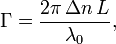
where λ0 is the vacuum wavelength of the light.
Half-wave plate

For a half-wave plate, the relationship between L, Δn, and λ0 is chosen so that the phase shift between polarization components is Γ = π. Now suppose a linearly polarized wave with polarization vector  is incident on the crystal. Let θ denote the angle between and
  , where is the vector along the waveplate's fast axis. Let z denote the propagation axis of the wave. The electric field of the incident wave is
is incident on the crystal. Let θ denote the angle between and , where is the vector along the waveplate's fast axis. Let z denote the propagation axis of the wave. The electric field of the incident wave is
where  lies along the waveplate's slow axis. The effect of the half-wave plate is to introduce a phase shift term eiΓ = eiπ = −1 between thef and s components of the wave, so that upon exiting the crystal the wave is now given by
lies along the waveplate's slow axis. The effect of the half-wave plate is to introduce a phase shift term eiΓ = eiπ = −1 between thef and s components of the wave, so that upon exiting the crystal the wave is now given by![E (\cos\theta\, \mathbf{\hat f} - \sin\theta\, \mathbf{\hat s})\mathrm{e}^{i(kz-\omega t)} = E [\cos(-\theta) \mathbf{\hat f} + \sin(-\theta) \mathbf{\hat s}]\mathrm{e}^{i(kz-\omega t)}.](https://upload.wikimedia.org/math/3/1/4/3145409fbe3b284da9098b1b956f793c.png)
If  denotes the polarization vector of the wave exiting the waveplate, then this expression shows that the angle between and is −θ. Evidently, the effect of the half-wave plate is to mirror the wave's polarization vector through the plane formed by the vectors and
  . For linearly polarized light, this is equivalent to saying that the effect of the half-wave plate is to rotate the polarization vector through an angle 2θ; however, for elliptically polarized light the half-wave plate also has the effect of inverting the light's handedness.[1]
denotes the polarization vector of the wave exiting the waveplate, then this expression shows that the angle between and is −θ. Evidently, the effect of the half-wave plate is to mirror the wave's polarization vector through the plane formed by the vectors and . For linearly polarized light, this is equivalent to saying that the effect of the half-wave plate is to rotate the polarization vector through an angle 2θ; however, for elliptically polarized light the half-wave plate also has the effect of inverting the light's handedness.[1]
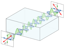
The half wave plate can be used to rotate the polarization state of a plane polarized light as shown in Figure 1.
 Suppose a plane-polarized wave is normally incident on a wave plate, and the plane of polarization is at an angle q with respect to the fast axis, as shown. After passing through the plate, the original plane wave has been rotated through an angle 2q.
A half-wave plate is very handy in rotating the plane of polarization from a polarized laser to any other desired plane (especially if the laser is too large to rotate). Most large ion lasers are vertically polarized. To obtain horizontal polarization, simply place a half-wave plate in the beam with its fast (or slow) axis 45° to the vertical. The l/2 plates can also change left circularly polarized light into right circularly polarized light or vice versa. The thickness of half waveplate is such that the phase difference is 1/2 wavelength (l/2, Zero order) or certain multiple of 1/2-wavelength [(2n+1)l/2, multiple order].
Quarter-wave plate


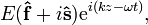
For a quarter-wave plate, the relationship between L, Δn, and λ0 is chosen so that the phase shift between polarization components is Γ = π/2. Now suppose a linearly polarized wave is incident on the crystal. This wave can be written as

where the f and s axes are the quarter-wave plate's fast and slow axes, respectively, the wave propagates along the z axis, and Ef and Esare real. The effect of the quarter-wave plate is to introduce a phase shift term eiΓ =eiπ/2 = i between the f and s components of the wave, so that upon exiting the crystal the wave is now given by

The wave is now elliptically polarized.
If the axis of polarization of the incident wave is chosen so that it makes a 45° with the fast and slow axes of the waveplate, then Ef = Es ≡E, and the resulting wave upon exiting the waveplate is
and the wave is circularly polarized.
Quarter wave plate are used to turn plane-polarized light into circularly  polarized light and vice versa. To do this, we must orient the wave plate so that equal amounts of fast and slow waves are excited. We may do this by orienting an incident plane-polarized wave at 45° to the fast (or slow) axis, as shown in Figure 2. When a l/4 plate is double passed, i.e., by mirror reflection, it acts as a l/2 plate and rotates the plane of polarization to a certain angle, i.e., 90°. This scheme is widely used in isolators, Q-switches, etc.
polarized light and vice versa. To do this, we must orient the wave plate so that equal amounts of fast and slow waves are excited. We may do this by orienting an incident plane-polarized wave at 45° to the fast (or slow) axis, as shown in Figure 2. When a l/4 plate is double passed, i.e., by mirror reflection, it acts as a l/2 plate and rotates the plane of polarization to a certain angle, i.e., 90°. This scheme is widely used in isolators, Q-switches, etc.
The thickness of the quarter waveplate is such that the phase difference is 1/4 wavelength (l/4, Zero order) or certain multiple of 1/4-wavelength [(2n+1)l/4, multiple order].
Quarter-Wave Plate Applications


The most common types of waveplates are quarter-wave plates (λ/4 plates) and half-wave plates (λ/2 plates), where the difference of phase delays between the two linear polarization directions is π/2 or π, respectively, corresponding to propagation phase shifts over a distance of λ / 4 or λ / 2, respectively.
Wave retarders are birefringent materials that alter (retard) the polarization state or phase of light traveling through them. A wave retarder has a fast (extraordinary) and slow (ordinary) axis.
As polarized light passes through a wave retarder, the light passing through the fast axis travels more quickly through the wave retarder than through the slow axis. In the case of a quarter wave retarder, the wave plate retards the velocity of one of the polarization components (x or y) one quarter of a wave out of phase from the other polarization component.
Polarized light passing through a quarter wave retarder thus becomes circularly polarized (see Figure 1). The action of the quarter wave is sometimes referred to as twisting or rotating the polarized light. Note that depending on which polarization component is retarded, one will have either a left handed or right handed circular polarizer.
Some important cases are:
- When a light beam is linearly polarized, and the polarization direction is along one of the axes of the waveplate, the polarization remains unchanged.
- When the incident polarization does not coincide with one of the axes, and the plate is a half-wave plate, then the polarization stays linear, but the polarization direction is rotated. For example, for an angle of 45° to the axes, the polarization direction is rotated by 90°.
- When the incident polarization is at an angle of 45° to the axes, a quarter-wave plate generates a state of circular polarization. (Other input polarizations lead to elliptical polarization states.) Conversely, circularly polarized light is converted into linearly polarized light.
Within a laser resonator, two quarter-wave plates around the gain medium are sometimes used for obtaining single-frequency operation(→ twisted-mode technique). Inserting a half-wave plate between a laser crystal and a resonator end mirror can help to reduce depolarization loss. The combination of a half-wave plate and a polarizer allows one to realize an output coupler with adjustable transmission.
Many waveplates are made of crystalline quartz (SiO2), as this material exhibits a wide wavelength range with very high transparency, and can be prepared with high optical quality. Other possible materials (to be used e.g. in other wavelength regions) are calcite (CaCO3), magnesium fluoride (MgF2), sapphire (Al2O3), mica (a silicate material), and some birefringent polymers.

Subscribe to:
Posts (Atom)
-
Diffraction Gating and Grating Spectrum and Polarization Diffraction Gating Diffraction Grating is optical device used to learn...
-
 FPGA demonstrates good performance and logic capacity by exploiting parallelism. At present single FPGA platform can play multi-functions,...
 -
LOGIC GATES:
